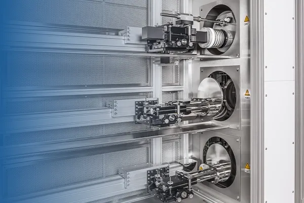
Tubestar
A Batch Type Tube furnace for RTP and deposition processes.
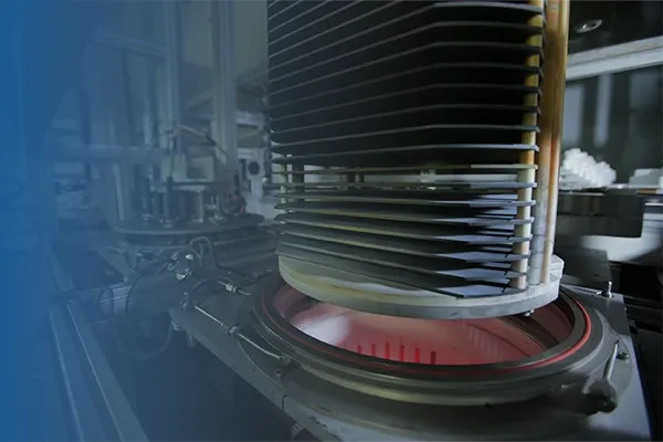
Memslab
PECVD Furnace for high quality thin film deposition.
Dry etching, or plasma etching, is an etching process that utilizes free radicals produced by plasma and particularly useful for materials and semiconductors which are chemically resistant and could not be wet etched.
Dry etching refers to the anisotropic removal of material, typically a masked pattern of semiconductor material, by exposing the material to a bombardment of ions that dislodge portions of the material from the exposed surface.
Opposite to wet texturing methods, plasma processes feature less dangerous handling, easier waste disposal, reduced use of reactants, consumables and water, and single-sided etching permitting new rear side concepts.
Do you have a question or a project ?
Would you like more information, to entrust us with a project or meet our teams ? Fill in our form and our teams will get back to you as soon as possible!